BOSTON, Oct. 31, 2023 /PRNewswire/ — Ensuring that sensitive electronic components are not adversely affected by radiated electromagnetic interference (EMI) is an essential part of circuit design. Where compactness and close component proximity are a priority, such as in smartphones and smartwatches, conventional board-level shielding with metallic enclosures is increasingly being replaced with conformal package-level shielding. This approach utilizes conductive coatings applied directly to semiconductor packages and, together with emerging deposition methods such as spraying and printing, creates new opportunities for functional materials.

When selecting a material for conformal package EMI shielding, a variety of factors need to be considered. Most important is the attenuation of incident electromagnetic radiation, which is a function of electrical conductivity and magnetic permeability. Often parametrized as shielding effectiveness (SE), higher values enable a thinner coating to be used, reducing weight and material consumption. Other material considerations include adhesion to the underlying epoxy molding compound of the package, thermal conductivity, density, chemical stability, and compatibility with the deposition method if solution processing.
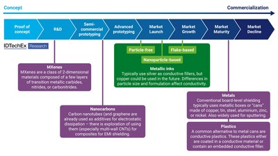
Concept to commercialization for EMI shielding. Source: IDTechEx
Sputtered metal
Sputtering metal is a well-established incumbent technology for conformal shielding, in which high-purity blocks of solid metal are ablated and deposited with a beam of charged ions. Many conformal shielding coatings use multiple metal layers, easily achieved by switching sputtering targets. Cap and/or adhesion layers are typically made from titanium, chromium, or stainless steel, with the primary shielding layer typically being cheaper metals such as copper, aluminum, or nickel.
While sputtering is well established, there is still scope for innovation. One proposed strategy, inspired by optical anti-reflective coatings, utilizes destructive interference from a multilayer stack to increase the shielding effectiveness. However, this improvement is highly frequency-dependent, given the fixed material spacing.
Conductive inks
Depositing conductive materials from solution provides an alternative to sputtering, with much-reduced equipment costs since the process occurs under ambient conditions rather than a vacuum. A range of solution processing methods, including spraying and inkjet printing, have been developed for EMI shielding, with all requiring conductive ink. Despite the high metal price, silver inks currently dominate due to their high conductivity and chemical stability.
Although the underlying metal is the same, there is extensive scope for differentiation amongst conductive ink suppliers. Particle shape and size are key factors, with nanoparticles generally offering higher conductivity but requiring higher curing temperatures than flake-based inks. Particle-free ink, also known as molecular ink, is a compelling emerging alternative. Rather than a suspension of metal particles, the ink is instead a solution of organometallic species that are reduced in situ, producing a smooth metal layer. A key advantage of particle-free conductive ink is eliminating the risk of nozzle clogging, a significant factor for digital printing methods such as aerosol and inkjet that enable selective deposition. Another benefit is that they produce very smooth coatings, which can improve shielding efficiencies at high frequencies.
MXenes
The ideal EMI shielding material would have high electrical conductivity, low density, flexibility to accommodate thermal expansion, tunable surface chemistry for adhesion, and solution processability. The emerging material class of MXenes, a family of two-dimensional inorganic materials composed of a few layers of transition metallic carbides, nitrides, or carbonitrides, fit this description. MXenes are thus the subject of both academic and commercial research for applications across electronics, including EMI shielding, with efforts currently being made to scale up production.
Comprehensive coverage
IDTechEx’s report “EMI Shielding for Electronics 2024-2034: Forecasts, Technologies, Applications” provides a detailed overview of the ‘EMI shielding for electronics’ market, with a more detailed assessment of the outlined materials classes along with nanocarbon-containing composites, metamaterials and combined thermal interface/EMI shielding materials. Innovations that will support the increasing adoption of heterogeneous integration and advanced semiconductor packaging, along with the activities of key players, are evaluated. 10-year forecasts for both deposition method and conductive ink consumption are provided, drawing on consumer electronic device analysis to assess the semiconductor package area requiring conformal shielding. Forecasts are segmented across multiple application categories, including smartphones, laptops, tablets, smartwatches, AR/VR devices, vehicles, and telecoms infrastructure.
For more information on this report, please visit www.IDTechEx.com/EMI, or for the full portfolio of related research available from IDTechEx please visit www.IDTechEx.com/Research/AM.
About IDTechEx
IDTechEx guides your strategic business decisions through its Research, Subscription and Consultancy products, helping you profit from emerging technologies. For more information, contact research@IDTechEx.com or visit www.IDTechEx.com.
Images download:
https://www.dropbox.com/scl/fo/rqkmylh1qki5lqhl33srb/h?rlkey=k1ub3tkzdg29yvsfqxa66qzyi&dl=0
Media Contact:
Lucy Rogers
Sales and Marketing Administrator
press@IDTechEx.com
+44(0)1223 812300
Social Media Links:
Twitter: www.twitter.com/IDTechEx
LinkedIn: www.linkedin.com/company/IDTechEx

Logo – https://mma.prnewswire.com/media/478371/IDTechEx_Logo.jpg
Photo – https://mma.prnewswire.com/media/2259004/IDTechEx_emi.jpg
![]() View original content:https://www.prnewswire.co.uk/news-releases/idtechex-evaluates-the-emerging-materials-landscape-for-emi-shielding-301969383.html
View original content:https://www.prnewswire.co.uk/news-releases/idtechex-evaluates-the-emerging-materials-landscape-for-emi-shielding-301969383.html

Featured image: DepositPhotos © Pkproject


